Design Single Digit Bcd Adder Using Ic 7483
BCD ADDER
BCD binary numbers represent Decimal digits 0 to 9. A 4-bit BCD code is used to
represent the ten numbers 0 to 9. Since the 4-bit Code allows 16 possibilities, therefore the
first 10 4-bit combinations are considered to be valid BCD combinations. The latter six
combinations are invalid and do not occur.
BCD Code has applications in Decimal Number display Systems such as Counters and
Digital Clocks. BCD Numbers can be added together using BCD Addition. BCD Addition is
similar to normal Binary Addition except for the case when sum of two BCD digits exceeds 9 or
a Carry is generated. When the Sum of two BCD numbers exceeds 9 or a Carry is generated
a 6 is added to convert the invalid number into a valid number. The carry generated by adding
a 6 to the invalid BDC digit is passed on to the next BCD digit.
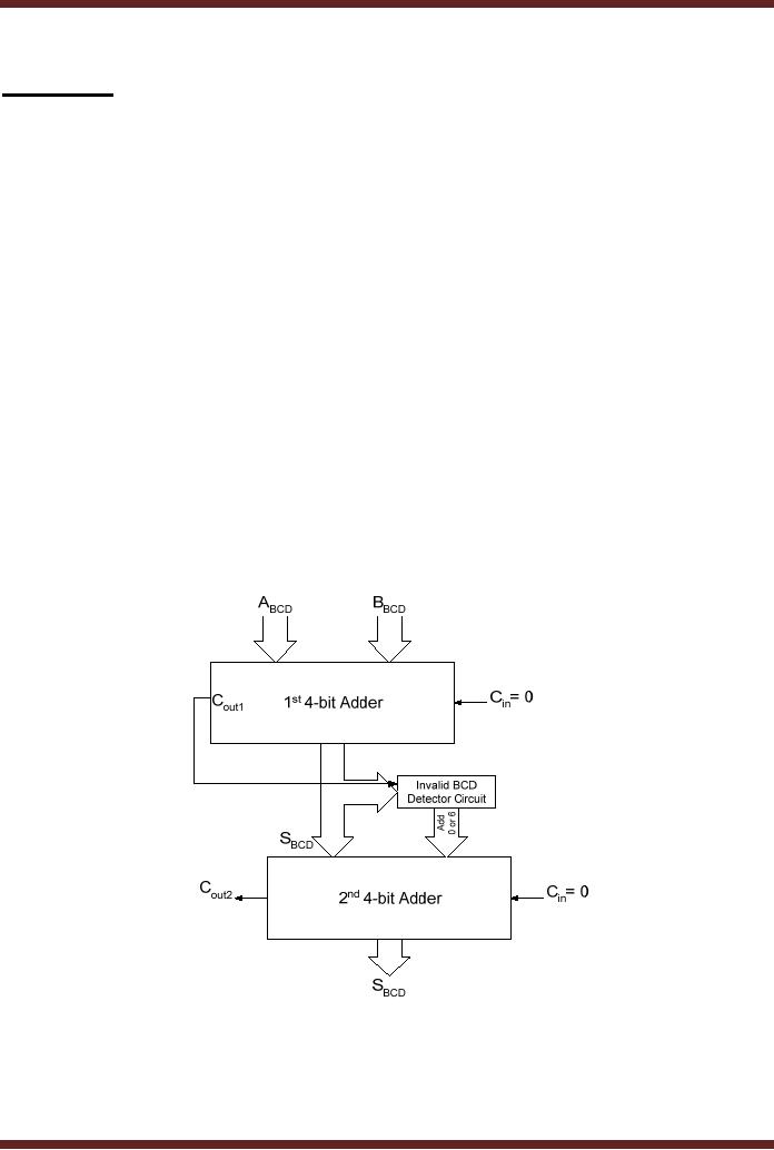
Addition of two BCD digits requires two 4-bit Parallel Adder Circuits. One 4-bit Parallel
Adder adds the two BCD digits. A BCD Adder uses a circuit which checks the result at the
output of the first adder circuit to determine if the result has exceeded 9 or a Carry has been
generated. If the circuit determines any of the two error conditions the circuit adds a 6 to the
original result using the second Adder circuit. The output of the second Adder gives the correct
BCD output. If the circuit finds the result of the first Adder circuit to be a valid BCD number
(between 0 and 9 and no Carry has been generated), the circuit adds a zero to the valid BCD
result using the second Adder. The output of the second Adder gives the same result. Figure
15.1
Figure 15.1
4-Bit BCD Adder
141
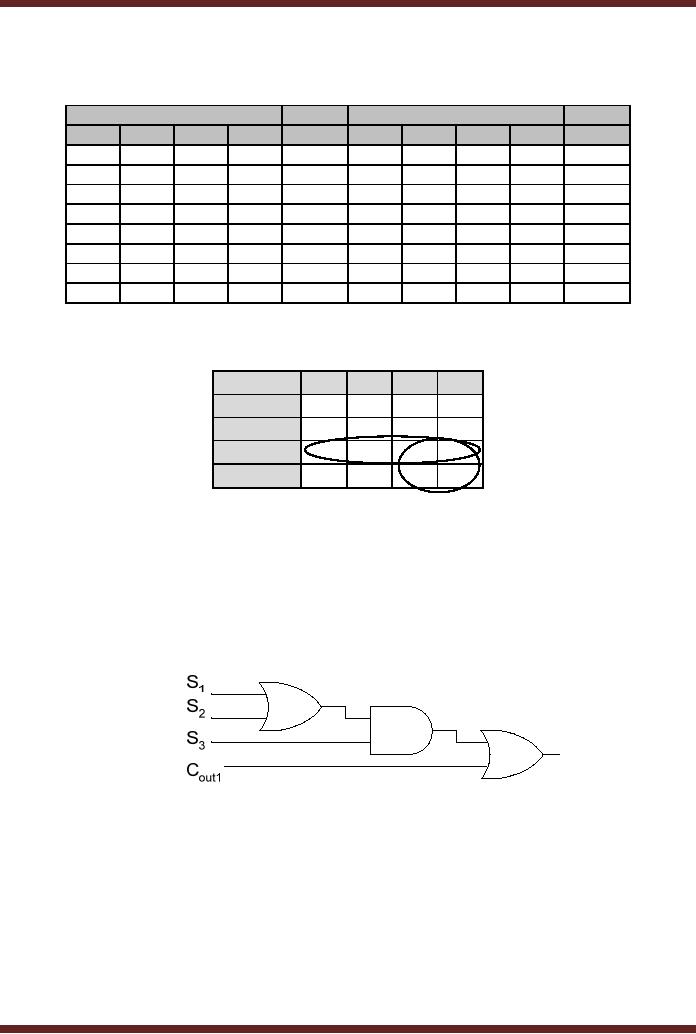
The circuit that checks if the output of the first Adder has exceeded 9 is a simple
combinational circuit with the function table specified. Table 15.1
Input
Output
Input
Output
S 3
S 2
S 1
S 0
F
S 3
S 2
S 1
S 0
F
0
0
0
0
0
1
0
0
0
0
0
0
0
1
0
1
0
0
1
0
0
0
1
0
0
1
0
1
0
1
0
0
1
1
0
1
0
1
1
1
0
1
0
0
0
1
1
0
0
1
0
1
0
1
0
1
1
0
1
1
0
1
1
0
0
1
1
1
0
1
0
1
1
1
0
1
1
1
1
1
Table 15.1
Function Table of Invalid BCD Number detector
S 3 S 2 \S 1 S 0
00
01
11
10
00
0
0
0
0
0
0
01
0
0
11
1
1
1
1
10
0
0
1
1
Figure 15.2
Mapping of Invalid BCD Number detector function
The Boolean expression for the Invalid BCD Number Detector obtained from the
Karnaugh Map which maps the function table is S 3 S 2 + S 3 S 1 = S 3 ( S 2 + S 1 )
The Invalid BCD Number is represented by two error conditions, either the BCD number is one
of the invalid numbers or a Carry out has been generated. Therefore the complete expression
for determining an incorrect BCD output is C out 1 + S 3 ( S 2 + S 1 ) . Figure 15.3
Figure 15.3
The Invalid BCD Detector Circuit
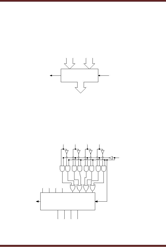
Connection of Invalid BCD Detector Circuit to second Adder
Adding of 6 when error conditions are detected and adding a zero when error
conditions are not detected is implemented by connecting the output of the Invalid BCD
Number Detector circuit to bits B 1 and B 2 of the Adder. Bits B 0 and B 3 are permanently
connected to 0. Figure 15.4. When an error condition is detected the output of the circuit is set
to logic 1, setting bits B 1 and B 2 to 1 and the 2 nd Adder input B to 0110. When the error
condition is not detected the circuit output is 0 and the 2 nd Adder input B is set to 0000.
142
Figure 15.4
Using the Second Adder to Add 6 or 0
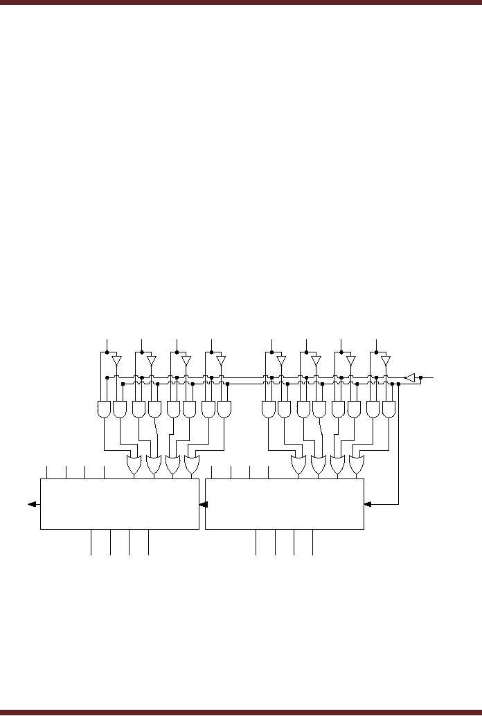
2-digit BCD Adder
Two singe digit BCD Adders can be cascaded together to form a 2-digit BCD Adder.
Four, 4-bit 74LS283 MSI chips are used. Two 74LS283s are required to directly add the two 2-
digit BCD numbers and the remaining two 74LS283s are required to add a six to the result if
any of the two digits add up to invalid BCD digits or generate a Carry. Two invalid BCD
detector circuits are used. Figure 15.5
A 4-7
B 4-7
A 0-3
B 0-3
C in4
C in = 0
1 st
1 st
MSD 4-bit Adder
LSD 4-bit Adder
C out8
C out4
Invalid BCD
Invalid BCD
Detector Circuit
Detector Circuit
S 4-7
S 0-3
0
0
0
0
C in4 =0
C in = 0
C out4
C out8
2 nd MSD 4-bit Adder
2 nd LSD 4-bit Adder
C out
S 4-7
S 0-3
Figure 15.5
2-Digit BCD Adder
Consider two examples. In the first example, 2-digit BCD number 99 is added with
another 2-digit BCD number 99. The answer should be 198 a 3-digit BCD number. Table 15.2.
In the second example, 2-digit BCD number 99 is added with another 2-digit BCD number 66.
The answer should be 165. Table 15.3
143
1 st MSD Adder
1 st LSD Adder
Carry
A(0-3)
1001
A(0-3)
1001
B(0-3)
1001
B(0-3)
1001
Cin4
1
Cin
0
S(0-3)
0011
S(0-3)
0010
Cout8
1
Cout4
1
Ckt. o/p 1
Ckt. o/p 1
2 nd LSD Adder
2 nd LSD Adder
A(0-3)
0011
A(0-3)
0010
B(0-3)
0110
B(0-3)
0110
Cin
0
Cin
0
1
S(0-3)
1001
S(0-3)
1000
Table 15.2
Adding BCD numbers 99 and 99
1 st MSD Adder
1 st LSD Adder
Carry
A(0-3)
1001
A(0-3)
1001
B(0-3)
0110
B(0-3)
0110
Cin4
1
Cin
0
S(0-3)
0000
S(0-3)
1111
Cout8
1
Cout4
0
Ckt. o/p 1
Ckt. o/p 1
2 nd LSD Adder
2 nd LSD Adder
A(0-3)
0000
A(0-3)
1111
B(0-3)
0110
B(0-3)
0110
Cin
0
Cin
0
1
S(0-3)
0110
S(0-3)
0101
Table 15.3
Adding BCD numbers 99 and 66
Subtraction
Subtraction in Digital Systems is performed by taking the 2's complement of the
number to be subtracted (subtrahend) and adding it to the minuend. The example shows the
subtraction of 6 represented in 2's complement form from nine also represented in its 2's
complement form. Since 9 is a positive number therefore its 2's complement representation is
the same. Neglecting the carry bit, the 4-bit number represents decimal 4.
9
1001
- 5
1011
4
1 0100
The 2's complement of any number is obtained by taking the 1's complement of a
number and then adding a 1 to the 1's complement. The two step process to represent a
negative number in its 2's complement form is shown
The number 5
0101
144
Invert all bits to result in 1's complement
1's complement of 5 is
1010
+1
2's complement of 5 is
1011
An Adder can be used to perform subtraction operations if the minuend is presented in
its 1's complemented form at the input of the adder circuit. The binary 1 that is added to the 1's
complement of a number to convert it into 2's complement is applied at the Carry In of the
Adder Circuit. Figure 15.6
1001
1010
A (0-3)
B (0-3)
Cout
Cin=1
4-bit Parallel
Adder
Sum (0-3)
Figure 15.6
4-bit Subtraction Circuit
The Adder circuit adds the number 9 (1001), 1's complement of 5 (1010) and the Carry
In which is set to 1.
A 4-bit bcd Adder/Subtracter Unit
An Adder can be connected to perform Additions and Subtractions by applying the un-
complemented and complemented data at one of the two inputs of the Adder respectively. The
Carry In input has also to be connected to 0 or 1 respectively. Figure 15.7
B 3
B 2
B 1
B 0
Add = 0
Subtract = 1
U
C
U
C
U
C
U
C
A 3 A 2 A 1 A 0
C In
C Out
4-bit Parallel Adder
S 3 S 2 S 1 S 0
Figure 25.7
4-bit Adder/Subtracter Unit
145
The AND gate and OR gate implementation connected at the B input of the 4-bit Adder
is used to allow Complemented or Un-Complemented B input to be connected to the Adder
input. Adding of two 4-bit numbers A and B can be performed by selecting the Add/Subtract =
0. The AND gates marked U (un-complemented) are enabled allowing B 0-3 to be passed on to
the OR gates and the B input of the Adder. Subtraction is performed by selecting the
Add/Subtract = 1. The AND gates marked C (complemented) are enabled allowing
complemented B 0-3 to be passed on to the OR gates and the B input of the Adder. The Carry
In is also set to 1 when Add/Subtract is set to 1.
An 8-bit bcd Adder/Subtracter Unit
Two 4-bit 74LS283 chips can be cascaded together to form an 8-bit Parallel Adder
Unit. Each of the two 74LS283 ICs is connected to the 1's Complement circuitry that allows
either the un-complemented form for addition or the complemented form for subtraction to be
applied at the B inputs of the two 74LS283s. Figure 15.8
The 8-bit Adder/Subtracter Circuit is similar to the 4-bit Adder/Subtracter Circuit. Two
sets of AND-OR based circuit that allows complemented and un-complemented B input to be
applied at the B inputs of the two 4-bit Adders. The Add/Subtract function select input are tied
together. The Carry In of the 1 st 4-bit Adder circuit is connected to the Add/Subtract function
select input. The Carry Out of the 1 st 4-bit Adder circuit is connected to the Carry In of the 2 nd
4-bit Adder circuit.
B 7
B 6
B 5
B 4
B 3
B 2
B 1
B 0
Add = 0
Subtract = 1
U
C
U
C
U
C
U
C
U
C
U
C
U
C
U
C
A 7 A 6 A 5 A 4
A 3 A 2 A 1 A 0
C In
C In
nd
1 st 4-bit Parallel Adder
2
4-bit Parallel Adder
C Out
S 7 S 6 S 5 S 4
S 3 S 2 S 1 S 0
Figure 15.8
8-bit Adder/Subtracter Circuit
Consider two number A=103 and B=67 which are first added and then subtracted using the 8-
bit Adder/Subtracter Circuit. Table 15.4 and Table 15.5
146
Adding 103 and 67
2 nd MS Adder
1 st LS Adder
Carry
A(4-7)
0110
A(0-3)
0111
B(4-7)
0100
B(0-3)
0011
Cin
0
Cin
0
0
S(4-7)
1010
S(0-3)
1010
Table 15.4
Adding 103 and 67
Subtracting 103 and 67
2 nd MS Adder
1 st LS Adder
Carry
A(4-7)
0110
A(0-3)
0111
B(4-7)
1011
B(0-3)
1100
Cin
1
Cin
1
1
S(4-7)
0010
S(0-3)
0100
Table 15.5
Subtracting 103 and 67
Arithmetic and Logic Unit (ALU)
Microprocessors have Arithmetic and Logic Units, a combinational circuit that can
perform any of the arithmetic operations and logic operations on two input values. The
operation to be performed is selected by set of inputs known as function select inputs.
There are different MSI ALUs available that have two 4-bit inputs a 4-bit output and
three to five function select inputs that allows up to 32 different functions to be performed.
Three commercially available 4-bit ALUS are
· 74XX181: The 4-bit ALU has five function select inputs allowing it to perform 32 different
Arithmetic and Logic operations.
· 74XX381: The 4-bit ALU only has three function select inputs allowing only 8 different
arithmetic and logic functions. Table 15.6
· 74XX382: The 4-bit ALU is similar to the 74XX381, the only difference is that 74XX 381
provides group-carry look-ahead outputs and 74XX382 provides ripple carry and overflow
outputs
Input
S2
S1
S0
Function
0
0
0
F=0000
0
0
1
F=B-A-1+C in
0
1
0
F=A-B-1+C in
0
1
1
F=A+B+C in
F = A ⊕ B
1
0
0
1
0
1
F=A+B
1
1
0
F=A.B
1
1
1
F=1111
147
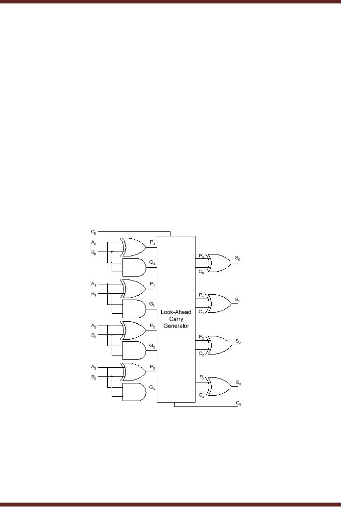
Table 15.6
Function Table of 74XX381 4-bit ALU
Implementing 16-bit ALU
16-bit ALU can be implemented by cascading together four 4-bit ALUs. These 4-bit
ALUs have built in Look-Ahead Carry Generator circuits that eliminate the delay caused by
carry bit propagating through the Parallel Adder circuit within the 4-bit ALU circut. However,
when a number of such units are cascaded together to implement large 16-bit and 32-bit ALU,
the carry propagating between one unit to the next gets delayed due to the Carry rippling
through multiple 4-bit units. For large 32-bit ALUs, the Carry propagates through 8, 4-bit units
delaying the Carry out from the last most significant unit by a factor of 8.The 74XX181 and
74XX381 circumvent the problem by having Group-Carry Look-Ahead.
Group-Carry Look-Ahead
The Look-Ahead Carry Generator discussed earlier and used by the 74LS283 Adder
provides Carry's C 1 , C 2 , C 3 and C 4 simultaneously after a gate delay of two. Carry's C 1 , C 2 and
C 3 are used internally, where as C 4 provides the C out from the 74LS283. Referring to the Look-
Ahead Carry Generator Circuit the C 1 , C 2 , C 3 and C 4 terms are generated on the basis of P 0 ,
P 1 , P 2 and P 3 the four Carry Propagate terms and G 0 , G 1 , G 2 and G 3 the four Carry Generate
terms. Figure 15.9
Figure 15.9
Look-Ahead Carry Generator
These terms are used to generate Group-Carry Look-Ahead outputs that can be used
to cascade together multiple units eliminating the problem of rippling carry. The G and P
output pins of the 74XX381 provide the group-carry look-ahead outputs that allow multiple
ALUs to be cascaded together. The active-low outputs G and P are represented by the
Boolean expressions. Figure 15.10
148

S0
S0
G
S1
S1
P
74X381
S2
S2
Cin
F4
A4
F0
A0
F5
B4
F1
B0
F6
A5
F2
A1
F7
B5
F3
B1
A6
A2
B6
B2
A7
A3
B7
B3
G = G 3 + P 3 G 2 + P 2 P 3 G 1 + P 1 P 2 P 3 G 0
P = P o P 1 P 2 P 3
Figure 15.10 74X381 ALU with Group-Carry Look-Ahead outputs
149
- AN OVERVIEW & NUMBER SYSTEMS
- Binary to Decimal to Binary conversion, Binary Arithmetic, 1�s & 2�s complement
- Range of Numbers and Overflow, Floating-Point, Hexadecimal Numbers
- Octal Numbers, Octal to Binary Decimal to Octal Conversion
- LOGIC GATES: AND Gate, OR Gate, NOT Gate, NAND Gate
- AND OR NAND XOR XNOR Gate Implementation and Applications
- DC Supply Voltage, TTL Logic Levels, Noise Margin, Power Dissipation
- Boolean Addition, Multiplication, Commutative Law, Associative Law, Distributive Law, Demorgan�s Theorems
- Simplification of Boolean Expression, Standard POS form, Minterms and Maxterms
- KARNAUGH MAP, Mapping a non-standard SOP Expression
- Converting between POS and SOP using the K-map
- COMPARATOR: Quine-McCluskey Simplification Method
- ODD-PRIME NUMBER DETECTOR, Combinational Circuit Implementation
- IMPLEMENTATION OF AN ODD-PARITY GENERATOR CIRCUIT
- BCD ADDER: 2-digit BCD Adder, A 4-bit Adder Subtracter Unit
- 16-BIT ALU, MSI 4-bit Comparator, Decoders
- BCD to 7-Segment Decoder, Decimal-to-BCD Encoder
- 2-INPUT 4-BIT MULTIPLEXER, 8, 16-Input Multiplexer, Logic Function Generator
- Applications of Demultiplexer, PROM, PLA, PAL, GAL
- OLMC Combinational Mode, Tri-State Buffers, The GAL16V8, Introduction to ABEL
- OLMC for GAL16V8, Tri-state Buffer and OLMC output pin
- Implementation of Quad MUX, Latches and Flip-Flops
- APPLICATION OF S-R LATCH, Edge-Triggered D Flip-Flop, J-K Flip-flop
- Data Storage using D-flip-flop, Synchronizing Asynchronous inputs using D flip-flop
- Dual Positive-Edge triggered D flip-flop, J-K flip-flop, Master-Slave Flip-Flops
- THE 555 TIMER: Race Conditions, Asynchronous, Ripple Counters
- Down Counter with truncated sequence, 4-bit Synchronous Decade Counter
- Mod-n Synchronous Counter, Cascading Counters, Up-Down Counter
- Integrated Circuit Up Down Decade Counter Design and Applications
- DIGITAL CLOCK: Clocked Synchronous State Machines
- NEXT-STATE TABLE: Flip-flop Transition Table, Karnaugh Maps
- D FLIP-FLOP BASED IMPLEMENTATION
- Moore Machine State Diagram, Mealy Machine State Diagram, Karnaugh Maps
- SHIFT REGISTERS: Serial In/Shift Left,Right/Serial Out Operation
- APPLICATIONS OF SHIFT REGISTERS: Serial-to-Parallel Converter
- Elevator Control System: Elevator State Diagram, State Table, Input and Output Signals, Input Latches
- Traffic Signal Control System: Switching of Traffic Lights, Inputs and Outputs, State Machine
- Traffic Signal Control System: EQUATION DEFINITION
- Memory Organization, Capacity, Density, Signals and Basic Operations, Read, Write, Address, data Signals
- Memory Read, Write Cycle, Synchronous Burst SRAM, Dynamic RAM
- Burst, Distributed Refresh, Types of DRAMs, ROM Read-Only Memory, Mask ROM
- First In-First Out (FIFO) Memory
- LAST IN-FIRST OUT (LIFO) MEMORY
- THE LOGIC BLOCK: Analogue to Digital Conversion, Logic Element, Look-Up Table
- SUCCESSIVE �APPROXIMATION ANALOGUE TO DIGITAL CONVERTER
Design Single Digit Bcd Adder Using Ic 7483
Source: https://zeepedia.com/read.php?bcd_adder_2-digit_bcd_adder_a_4-bit_adder_subtracter_unit_digital_logic_design&b=9&c=15
0 Response to "Design Single Digit Bcd Adder Using Ic 7483"
Post a Comment